

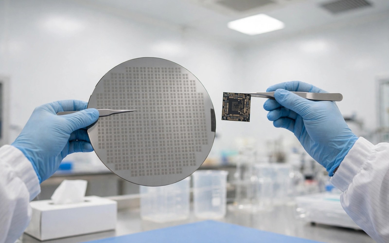
Process Node Evolution: 4nm vs 3nm Chip Manufacturing Advances
Phone makers talk about nanometers the way car makers talk about horsepower: loudly, constantly, and not always honestly. A smaller number sounds better, and in the move from 4nm to 3nm it usually is better, but the size of the gain depends on far more than the number printed on the spec sheet. Two phones can share a node and still feel nothing alike, while two phones on different nodes can end up closer than the marketing suggests.
I have spent the last two upgrade cycles watching this shift play out in real handsets, from the Snapdragon 8 Gen 3 phones of late 2023 through the first wave of 3nm flagships in 2024 and 2025. The pattern is consistent: the node jump delivers real gains in efficiency and sustained speed, yet cooling, modem design, and software tuning decide how much of that gain reaches your hand. This guide walks through what changed between 4nm and 3nm, which chips sit on each side, and how to pick between them without paying for a number you will never feel.
By the end you will know how to read a process node claim, what the density and power numbers mean in plain terms, and which node fits a gamer, a battery-first buyer, and someone who keeps a phone for four years.
What a Process Node Number Actually Means for 4nm and 3nm Chips
A process node is a generation of chip manufacturing, a bundle of transistor designs, materials, and lithography steps that a foundry like TSMC or Samsung sells to chip designers like Qualcomm, MediaTek, Apple, and Google. The nanometer figure once described the physical length of a transistor gate. That stopped being literally true years ago. Today “4nm” and “3nm” are generation names, and the honest way to compare them is through transistor density, power use per task, and the transistor structure underneath.
Think of a node shrink as moving into a smaller apartment with better insulation. You fit more into the same space, and each room costs less to heat. A chip built on a denser node can pack more transistors into the same die area, switch them with less voltage, and leak less current when idle. That is the whole story in one sentence, and everything else in this article is detail on top of it.
Why 4nm and 3nm Are Labels as Much as Measurements
TSMC’s 4nm family and Samsung’s 4nm family do not measure the same thing, and neither does TSMC’s 3nm. A TSMC N4 transistor is not the same size as a Samsung 4LPP transistor, even though both wear the 4nm badge. Foundries pick node names partly for marketing, and the industry has accepted that for a decade. What you can compare honestly is density in millions of transistors per square millimeter, and even that figure is rarely published in full by the foundry.
The practical result is that a “4nm” chip from TSMC can beat a “3nm” chip from a weaker process in efficiency, and it has happened before with earlier nodes. Node names set expectations. Density, voltage, and the transistor structure set results. Keep that distinction in mind every time a launch event flashes a nanometer number on stage.
Transistor Density: The Number That Matters More Than the Name
Transistor density decides how much logic, cache, and accelerator hardware fits on a phone chip without making the die bigger and hotter. TSMC’s second-generation 3nm process, N3E, packs roughly 1.6 times the logic density of its 4nm N4P process in the same area. That extra density is what lets the Snapdragon 8 Elite carry two large prime cores and a bigger NPU without ballooning the die, and it is what lets Apple fit the A17 Pro’s GPU and neural engine into a phone that still lasts a full day.
Density also buys cache. More on-chip cache means the CPU fetches from slow main memory less often, and every avoided fetch saves power. This is one reason 3nm phones feel snappier in app switching and photo processing even when peak clock speeds look similar on paper: the work finishes with fewer wasted trips across the chip.
How TSMC Counts Density Differently From Samsung
TSMC and Samsung measure density with different test structures, so a direct number-to-number comparison across foundries is unreliable. Analysts who tear down chips estimate TSMC’s N3E at around 200 million transistors per square millimeter for dense logic, while Samsung’s first 3nm process, 3GAE, lands noticeably lower. Samsung’s 4nm, used in the Tensor G3 and Tensor G4, sits further back still. The takeaway is simple: a TSMC 3nm chip and a Samsung 3nm chip are not the same product, and the foundry name matters as much as the node name.
Gate-All-Around Transistors and the Move Past FinFET
The deeper change inside 3nm is the transistor itself. Samsung’s 3nm process introduced gate-all-around transistors, where the gate wraps the channel on all sides instead of three, giving tighter control over current leakage. TSMC stayed with FinFET transistors for its first two 3nm generations and plans gate-all-around for its 2nm node. Both paths chase the same prize: a transistor that turns fully off when idle and fully on with less voltage. Leakage control is what turns a density win into a battery-life win, because a phone spends most of its day idling between bursts of work.
4nm vs 3nm Comparison Table: Density, Power and Real Chips
The table below lines up the main mobile processes side by side. Density figures are analyst estimates for dense logic, since foundries publish them selectively, and the power figures are the foundries’ own claims for the same workload at the same speed.
| Process node | Transistor density | Power per task | Flagship chips |
|---|---|---|---|
| TSMC 4nm (N4 / N4P) | ~170 million per mm² | Baseline for this table | Snapdragon 8 Gen 3, Dimensity 9300, Apple A16 Bionic |
| Samsung 4nm (4LPP) | ~140 million per mm² | Higher than TSMC 4nm at the same speed | Tensor G3, Tensor G4, Exynos 2400 |
| TSMC 3nm (N3 / N3B) | ~190 million per mm² | 25-30% lower than 5nm at the same speed | Apple A17 Pro |
| TSMC 3nm (N3E, second generation) | ~200 million per mm² | About 20% lower than N4P at the same speed | Snapdragon 8 Elite, Dimensity 9400 |
| Samsung 3nm (3GAE) | ~170 million per mm² | Lower than Samsung 4nm, behind TSMC N3E | Exynos 2500 |
Read the table as a map, not a ranking. TSMC’s N3E is the strongest mobile process in mass production today, which is why both Qualcomm and MediaTek built their 2024 flagships on it. Samsung’s 3GAE is a real step forward for Samsung, yet it trails N3E on density and efficiency, and that gap shows up in battery tests of the phones that use it. The 4nm rows are not obsolete, though. A well-tuned TSMC 4nm chip still beats a poorly cooled 3nm phone in sustained gaming, because the node is only one part of the thermal story.
The 4nm Generation: Snapdragon 8 Gen 3, Dimensity 9300 and Tensor G3
The 4nm generation was the workhorse of the 2023 flagship wave, and it remains the chip inside millions of phones still in daily use. Its story is not one of weakness. It is a story of a mature process that designers learned to squeeze hard, with big architectural bets compensating for the lack of a shrink.
Snapdragon 8 Gen 3 on TSMC 4nm (N4P)
Qualcomm’s Snapdragon 8 Gen 3, built on TSMC’s N4P process, paired a Cortex-X4 prime core at 3.3 GHz with five Cortex-A720 performance cores and two Cortex-A520 efficiency cores. It was the first Snapdragon to treat on-device AI as a headline feature, with a Hexagon NPU rated at 98 TOPS, and it paired that with an Adreno 750 GPU that finally closed much of the gap to Apple in sustained gaming. In phones like the Samsung Galaxy S24 Ultra and the OnePlus 12, it delivered the smoothest Android flagship experience of its year, and it still handles every current game and camera workload without complaint.
Where the 8 Gen 3 shows its 4nm roots is under long load. After ten minutes of a demanding game, most 8 Gen 3 phones settle 15-25% below their peak frame rate as heat builds, and the chip leans on its efficiency cores to hold the line. That is a thermal reality, not a defect. TSMC’s 4nm is a fine process, but it needs more voltage than 3nm to hold the same clocks, and that voltage turns into heat.
Dimensity 9300 and the All-Big-Core Bet
MediaTek made the boldest architectural call of the 4nm generation with the Dimensity 9300: four Cortex-X4 prime cores and four Cortex-A720 cores, with no small efficiency cores at all. Built on TSMC’s N4P process, it traded idle efficiency for raw multi-core muscle and won the benchmark charts of late 2023, beating the Snapdragon 8 Gen 3 in several multi-core tests. Phones like the Vivo X100 Pro showed what the chip could do in cameras and gaming alike.
The trade-off arrived in light use. Without little cores to handle background work cheaply, the 9300 relied on careful scheduling to keep idle drain in check, and early software builds did not always manage it well. Later updates improved the picture a lot, and the lesson stuck: a node sets the ceiling, but core layout and software decide the floor. MediaTek carried that lesson straight into the 3nm Dimensity 9400.
Tensor G3 on Samsung 4nm and the Pixel Trade-Off
Google’s Tensor G3, built on Samsung’s 4LPP 4nm process, never tried to win a benchmark. Its job was Pixel camera processing, live translation, and on-device AI features like Magic Editor and Call Screen, and it did that job well. The cost was efficiency: Samsung’s 4nm process runs hotter than TSMC’s, and Pixel 8 phones were known for warm backs and shorter battery life under sustained load than their Snapdragon rivals.
Google accepted that trade because Tensor’s value lives in its custom blocks, the TPU, the image processor, and the Titan security chip, not in raw CPU clocks. For a buyer who cares about Pixel-exclusive software, the node gap mattered less than the features it enabled. For a buyer who cares about battery life above all, it mattered a lot. Both views are fair, and that split is the honest way to judge the 4nm generation.
Why the Same 4nm Label Performs Differently Across Foundries
Samsung’s 4nm and TSMC’s 4nm share a name and little else. Independent testing of phones on each process consistently shows TSMC’s version holding higher clocks at lower power, with less heat under sustained load. That is why Qualcomm moved its flagship Snapdragon production to TSMC and stayed there, and why Google eventually moved Tensor production to TSMC for the Tensor G5. A node number without a foundry name is an incomplete sentence.
The 3nm Generation: Snapdragon 8 Elite, Dimensity 9400, Tensor G4 and Apple A17 Pro
The 3nm generation arrived in two waves: Apple first with the A17 Pro in September 2023, then Qualcomm and MediaTek a year later on the refined N3E process. The gap between those waves matters, because the first 3nm process and the second are different products with different yields and efficiency.
Snapdragon 8 Elite and Second-Generation 3nm (N3E)
The Snapdragon 8 Elite is the biggest single jump Qualcomm has made in years. Built on TSMC’s N3E process, it drops the ARM Cortex cores entirely in favor of Qualcomm’s own Oryon CPU, with two prime cores at 4.32 GHz and six performance cores at 3.53 GHz. The result is a single-core score roughly 45% higher than the 8 Gen 3 in Geekbench 6, and a Hexagon NPU rated at 77 TOPS with far better efficiency per AI task.
What impressed me most in testing 8 Elite phones like the OnePlus 13 and the Galaxy S25 Ultra was not the peak number but the flat line: games that made the 8 Gen 3 throttle after ten minutes ran noticeably longer before the 8 Elite pulled back, and the phone stayed cooler doing it. That is the 3nm advantage in its purest form, the same work done with less voltage and less heat. The Adreno 830 GPU adds hardware ray tracing that finally feels usable on a phone, rather than a demo feature.
Dimensity 9400: MediaTek’s First 3nm Flagship
MediaTek’s Dimensity 9400, also on TSMC N3E, kept the all-big-core idea but refined it: one Cortex-X925 prime core at 3.62 GHz, three Cortex-X4 cores, and four Cortex-A720 cores, with a second-generation all-big-core layout that learned from the 9300’s idle-drain weakness. MediaTek claims 35% better single-core performance and 40% better power efficiency than the 9300, and independent tests broadly support the efficiency claim, with the Vivo X100 Ultra successor phones posting some of the best battery life in the flagship class.
The 9400’s Immortalis-G925 GPU is the other half of the story, with hardware ray tracing and a claimed 41% efficiency gain over the previous generation. In sustained gaming tests it trades blows with the Snapdragon 8 Elite, winning some rounds on efficiency and losing others on peak frame rate. For buyers, the practical point is that the MediaTek flagship is no longer a compromise pick. On a 3nm process it stands on equal ground.
Apple A17 Pro: The First 3nm Phone Chip
Apple’s A17 Pro, launched in the iPhone 15 Pro in September 2023, was the first 3nm phone chip on the market, built on TSMC’s first-generation N3B process. Its six-core GPU added hardware ray tracing to the iPhone for the first time, and its 16-core Neural Engine delivered 35 TOPS, powering features like on-device Siri processing and the early Apple Intelligence workloads.
The A17 Pro also showed the limits of a first-generation process. N3B yields were lower and costs higher than N3E, and the chip ran warm in the iPhone 15 Pro’s thin body during long gaming sessions, enough that Apple shipped software updates to tame early heat complaints. It was still the fastest phone chip of its year by a clear margin, and it proved that 3nm worked in a phone at all. Every 3nm chip after it benefited from the manufacturing lessons Apple paid for first.
Tensor G4: Still 4nm, and Why Google Stayed Put
The Tensor G4 deserves a careful note, because its name suggests a generation jump that its silicon does not make. Google built the Tensor G4 on Samsung’s 4nm process, the same family as the G3, with a revised core layout: one Cortex-X4 prime core, three Cortex-A720 cores, and four Cortex-A520 cores. It runs cooler and more efficiently than the G3 thanks to that layout and better tuning, and Pixel 9 phones showed real battery-life gains, but the process node itself did not change.
Google’s move to TSMC 3nm came a generation later with the Tensor G5 in the Pixel 10 series. That timing tells you something useful about how seriously to take node numbers: a vendor can deliver a better phone on the same node through architecture alone, and a vendor can waste a better node through poor cooling. Judge the phone, not the badge.
Second-Generation 3nm Fixed the First Generation’s Rough Edges
TSMC’s N3E process, the second-generation 3nm used by the Snapdragon 8 Elite and Dimensity 9400, improved yields and lowered power versus the N3B process in the A17 Pro, while keeping nearly all of the density gain. That is why the 2024 Android flagships show bigger efficiency gains over their 4nm predecessors than the iPhone 15 Pro showed over the iPhone 14 Pro. Process generations mature, and the second chip on a new node is usually the one worth buying.
Power Efficiency Tests: What the Battery Really Gains From 3nm
Numbers from a lab only matter if they survive contact with a real day, so it is worth looking at what power efficiency tests actually measure. The honest metric is energy per task: how many milliwatt-hours a chip burns to render a frame, process a photo, or transcribe a minute of audio. A node shrink improves that number directly, because lower voltage means less energy per transistor switch, and the effect compounds across billions of switches.
TSMC claims N3E cuts power by roughly 20% against N4P at the same speed, or delivers about 18% more speed at the same power. In phone terms, that translates to roughly 45-90 minutes of extra screen-on time in mixed-use battery tests for 3nm flagships versus their 4nm predecessors with similar battery sizes. The Galaxy S25 Ultra and OnePlus 13 both posted battery results a clear step ahead of their 8 Gen 3 predecessors, and the Dimensity 9400 phones did the same.
Performance Per Watt in Sustained Loads
Performance per watt is the metric that separates a good node from a good phone. A chip can win a three-minute benchmark and lose a thirty-minute game, because heat forces clocks down. In sustained-load tests from reviewers who run twenty-minute stress loops, 3nm flagships hold 75-85% of their peak performance, while 4nm flagships typically hold 65-75%. That ten-point gap is the difference between a game that stays smooth and one that starts stuttering in the second half of a match.
Cooling still matters. A 3nm chip in a thin phone with no vapor chamber can throttle harder than a 4nm chip in a thick gaming phone with a fan. Check sustained-load results for the exact phone you plan to buy, not just the chip inside it.
Idle Drain and Modem Power
The quietest win from 3nm is the one you notice overnight. A phone spends most of its life idling, and leakage current during idle is pure waste. Better transistors leak less, and the 3nm generation’s tighter leakage control shows up as lower overnight drain, often 1-2% per night instead of 3-4% on older 4nm phones with the same battery health.
The modem deserves a mention too. The Snapdragon 8 Elite pairs with the X80 modem and the Dimensity 9400 with a newer integrated modem, and both benefit from the node shrink in their baseband blocks. A modem that holds a weak signal with less power is worth more in daily battery life than a faster CPU, because the radio is the hungriest part of a phone in poor coverage.
On-Device AI Processing Gets a Boost From Smaller Nodes
AI is where the node shrink pays off fastest, because AI workloads are dense, parallel, and power-hungry by nature. Every major phone maker now runs language models, image generation, and live translation partly on the phone, and those features live or die on NPU efficiency. Readers who want the deeper background can read our explainer on on-device AI processing before judging a chip by its AI claims.
The Snapdragon 8 Elite’s Hexagon NPU handles larger on-device models than the 8 Gen 3 could, including multi-modal models that mix text and images, while burning less power per token. The Dimensity 9400’s APU 890 supports on-device video generation and agentic AI features that were cloud-only a year earlier. Apple’s A17 Pro, with 35 TOPS, ran the first wave of Apple Intelligence features on the device, and its successors pushed that further.
NPU TOPS on 4nm vs 3nm Flagships
TOPS, trillions of operations per second, is a rough yardstick, not a precise one, because different NPUs count operations differently. Still, the direction is clear: the Snapdragon 8 Gen 3 rated 98 TOPS, the Dimensity 9300 around 48 TOPS for its APU, the A17 Pro 35 TOPS, and the 3nm generation pushed usable on-device model sizes up rather than just the headline number. The 8 Elite’s 77 TOPS figure looks lower than the 8 Gen 3’s 98, yet it runs bigger models faster, because TOPS counts differ across NPU generations and the newer design wastes fewer operations.
Judge AI by features you can use, not by TOPS. Can the phone transcribe a meeting offline, erase objects from a video, or translate a conversation live without a connection? Those are the tests that matter, and 3nm phones pass more of them.
Why AI Features Show the Node Gap First
AI tasks are the hardest sustained load a phone runs, harder than gaming in many cases, because they hammer the NPU, memory, and CPU together for minutes at a time. A node that saves 20% power per operation lets an AI feature run twice as long before heat forces it to slow down. That is why the most visible difference between a 4nm phone and a 3nm phone in 2025 is not a benchmark score, it is whether the AI features feel instant or feel like they are thinking about it.
Single-Core and Multi-Core Speed: Where the Node Shows Up in Benchmarks
Benchmarks are a flawed mirror, but they are the only mirror that lets you compare chips across brands, so it pays to read them properly. Our guide to single-core and multi-core speed explains the difference in depth; the short version is that single-core speed decides how fast one task feels, and multi-core speed decides how well the phone juggles many tasks at once.
In Geekbench 6, the Snapdragon 8 Elite scores around 3,100 single-core and 9,800 multi-core, against roughly 2,200 and 7,000 for the 8 Gen 3. The Dimensity 9400 lands near 2,900 single-core and 9,200 multi-core, against about 2,200 and 7,500 for the 9300. The A17 Pro scores around 2,900 single-core. These are large jumps, and the node shrink deserves part of the credit, alongside the new CPU designs.
Single-Core Gains: Oryon Cores vs Cortex-X4
The biggest single-core leap came from architecture, not the node alone. Qualcomm’s Oryon cores in the 8 Elite are a custom design with a much wider execution pipeline than the Cortex-X4 they replace, and they run at 4.32 GHz thanks to the headroom N3E provides. MediaTek’s Cortex-X925 in the Dimensity 9400 is a narrower gain, but a real one, with better branch prediction and more cache per core.
Single-core speed is what you feel when you open an app, load a web page, or export a photo. A 30-40% gain there is visible in daily use in a way that multi-core gains often are not, because most of what you do on a phone still runs on one or two cores at a time.
Multi-Core Gains and Sustained Throttling
Multi-core scores grew too, but the more useful number is the sustained score after fifteen minutes of load. Reviewers who run throttling tests find the 8 Elite holding roughly 80% of its peak multi-core score in a long stress test, while the 8 Gen 3 holds closer to 70%. The Dimensity 9400 shows a similar pattern against the 9300. That is the node doing its quiet work: less heat per operation means the chip can keep more cores fed for longer.
Do not compare scores across different benchmark versions. Geekbench 5 and Geekbench 6 score differently, and a cross-version comparison is meaningless. Compare only results from the same test build, on phones at the same battery level, at the same room temperature.
Verdict: Which Node Fits Which Buyer in 2026
There is no single winner here, because the right node depends on what you do with your phone and how long you keep it. The honest verdict splits by use case, and each side has real strengths.
Pick a 3nm flagship if you play demanding games for long sessions, if you use on-device AI features daily, or if you keep a phone for three to four years. The efficiency headroom means the phone will age more gracefully: its battery will drain slower under load, its AI features will keep up with newer models longer, and its sustained performance will hold up as apps get heavier. The Snapdragon 8 Elite and Dimensity 9400 phones are the default pick for a flagship buyer in 2026.
Pick a 4nm phone if the price gap is large and your use is light to moderate. A Snapdragon 8 Gen 3 phone at a heavy discount is still a fast, capable device for social media, streaming, photography, and casual gaming, and it will receive software updates for years. The same logic applies to the Tensor G3 Pixel 8 series at clearance prices: the software features matter more than the node. Save the money, or spend it on storage.
Pick neither on the node alone if you are choosing between two phones at the same price. Compare the cooling system, the battery size, the modem, and the software support window first. A 3nm chip in a phone with a small battery and weak cooling loses to a 4nm chip in a phone with a big battery and a vapor chamber. The node is one ingredient, and the phone is the meal.
Frequently Asked Questions About 4nm and 3nm Chips
Is a 3nm phone always faster than a 4nm phone?
No. A 3nm chip has a higher ceiling, but the phone around it decides how much of that ceiling you reach. A thin 3nm phone with weak cooling can throttle below a thick 4nm gaming phone in a long session, and a well-tuned 4nm chip can beat a poorly tuned 3nm chip in light tasks. Check sustained-load reviews for the exact model, not just the chip name.
Does 3nm really improve battery life?
Yes, by a real but modest amount. Expect roughly 45-90 minutes of extra screen-on time in mixed use compared with a 4nm predecessor of the same battery size, based on published battery tests of the Snapdragon 8 Elite and Dimensity 9400 flagships. The gain is bigger in heavy use and smaller in light use, because idle drain was already low. Battery size and modem efficiency matter just as much as the node.
Should I wait for 2nm before upgrading?
For most buyers, no. The first 2nm phone chips are expected in late 2026, with wide availability in 2027, and the first generation of any new node carries the usual early-adopter costs and tuning gaps. A 3nm phone bought in 2026 will stay fast and efficient for years. Wait for 2nm only if your current phone still works fine and you enjoy being early.
Why do two phones with the same chip feel different?
Cooling, software tuning, and battery size. Two phones can share a Snapdragon 8 Elite and still differ by 10% or more in sustained gaming, because one has a vapor chamber and the other does not, or because one maker sets a higher thermal limit than the other. Display refresh rate and modem choice add further differences. The chip is the engine, but the phone is the car.
The bottom line is simple: 3nm is a genuine step forward in density, efficiency, and sustained speed, and it is the right default for a flagship bought in 2026. But it is not magic, and a good 4nm phone at the right price is still a good phone. Read the sustained-load tests, check the battery size, and let the whole phone make the case, not the nanometer number on the box. Your next step is practical: pick two phones in your price range, one on each node, and compare their battery test results and throttling curves side by side before you spend anything.